Chapter 5
RC and RL First-Order Circuits
m5.3 Response of the RC Circuit
Figure m5.3a shows a resistor-capacitor circuit with a pair of switches and
Figure m5.3a shows the switch opening-closing behavior as a function of time.
The initial capacitor voltage is -9 V. Component values are R1 = 10 kΩ,
R2 = 3.3 kΩ, and R3 = 2.2 kΩ, C = 1.0 μF, V 1 = 9 V and V 2 = -15 V.
- Determine the equation that describes v(t) over the time range 0 to
50 ms.
- Plot v(t) over the time range 0 to 50 ms.
- Determine the values of v(t) at the times 5, 15, 25, 35, and 45 ms.
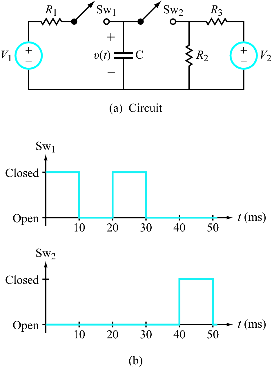
Figure m5.3: Circuit for Problem m5.3
NI Multisim Measurements
- Enter the circuit of Figure m5.3a using the following components:
- VOLTAGE_CONTROLLED_SWITCH
- ABM_VOLTAGE (Analog Behavioral Modeling) voltage source;
use step functions (u(TIME)) to create the switch control
waveforms of Figure m5.3b.
- Capacitor with initial value of -9 volts.
- Name the net that connects the two switches to the capacitor. Set up a
Simulate → Analyses → Transient analysis with the end time set to 0.05
seconds and with “Initial Conditions” set to “User-defined.” Select the
“Output” tab and add the capacitor voltage to the list of analysis variables.
Run the simulator to plot v(t).
- Use the oscilloscope cursor to measure the values of v(t) at the times 5, 15,
25, 35, and 45 ms.
NI Multisim video tutorials:
NI myDAQ Measurements
- Construct the circuit of Figure m5.3a using the following
components and NI ELVISmx instruments:
- Two normally-open Switches 1 and 4 contained in the Intersil
DG413 quad analog switch described in
Appendix D. Refer to
the pinout diagram of Figure D.1 and connect power according
to the photograph of Figure D.2.
- 9.0 volt source created with the LM317 variable voltage circuit
of Figure B.2 in Appendix B.
- 1.0 μF electrolytic capacitor. Connect the negative terminal of
the capacitor to ground.
- AO0 (Analog Output 0) to the switch control input of Switch 1.
- AO1 (Analog Output 1) to the switch control input of Switch 4.
- AI0 (Analog Input 0) to display the switch control voltage for
Switch 1; connect AI0+ to the switch control input and connect
AI0- to ground.
- AI1 (Analog Input 1) to display the capacitor voltage v(t);
connect AI1+ to the positive side of the electrolytic capacitor and
connect AI1- to ground.
- Arbitrary Waveform Generator to create the switch control
waveforms of Figure 5.3b.
- Oscilloscope to view the Switch 1 control waveform and the
capacitor voltage v(t). Adjust the Oscilloscope settings to
display the voltage v(t) so that the waveform fills a reasonable
amount of the available display. Use a combination of edge
triggering and the “Horizontal Position” control. You may find
it helpful to set the “Acquisition Mode” to “Run Once” and then
click the “Run” button repeatedly until you capture a good trace.
- Use the oscilloscope cursor to measure the values of v(t) at the times 5, 5,
25, 35, and 45 ms.
NI myDAQ video tutorials:
Further Exploration with NI myDAQ
The circuit of Figure m5.3a permits the capacitor to be charged to a desired
voltage by closing one of the switches that connects the capacitor to a source.
After charging, opening both switches should in principle allow the capacitor to
maintain its “charge” (or stored energy) indefinitely. However, the physical
capacitor contains a nonideal dielectric material between its plates that allows a
slow trickle of current that eventually depletes the stored energy. The
nonideal dielectric can be modeled as a resistor in parallel with the capacitor
plates.
Devise a method to estimate the value of the equivalent resistance that
connects the capacitor plates. Consider the half-life measurement technique of
Figure E.1 in Appendix E
to measure the time constant. Connect the switch control inputs to
DIO0 and DIO1 and use the NI ELVISmx Digital Writer to manually operate the
switches. Use NI ELVISmx Oscilloscope to display the capacitor voltage, taking
special care to enable only one active oscilloscope channel. Enabling both
oscilloscope channels greatly reduces the effective input resistance of the
myDAQ analog inputs due to the rapid switching between these channels to a
common analog-to-digital converter.